By Aman Yadav — Kindastuff Solar Analytics
Category: Solar O&M — Inverter Diagnostics | Reading time: ~10 min |
IGBT Failure in Utility-Scale Solar Inverters: What Field Failure Actually Looks Like — and How It Degrades Inverter Efficiency, PR, and CUF
The charring was visible the moment the panel came off. The gate driver PCB adjacent to one of the power modules was blackened from the inside out. The IGBT had not just failed — it had vented. The central inverter had been logging an IGBT fault alarm on and off for two days before the unit fully tripped offline. By the time the root cause was confirmed, the plant had lost a measurable block of generation that showed up directly in that month’s Performance Ratio report.
If you manage utility-scale solar assets, you will encounter this. What you may not know is what the inverter was doing in the hours and days before that fault alarm appeared — and how much performance loss had already accumulated before anyone responded.
This article covers what IGBTs actually do inside a central inverter, why they fail under field conditions, and how to read the performance data that appears before, during, and after a failure. No datasheet theory. No generic switching diagrams. What follows is grounded in field evidence from utility-scale plant operations.
What IGBT Does Inside a Central Solar Inverter
An Insulated Gate Bipolar Transistor (IGBT) is the power switching device at the core of every solar inverter’s power conversion stage. In a central inverter, you will not find a single IGBT — you will find them arranged in a three-phase bridge configuration, typically as a set of six IGBT modules (two per phase leg), each handling a portion of the full DC current from your PV array.
Their job: switch at high frequency — typically 2–5 kHz for utility-scale central inverters, depending on inverter topology and manufacturer design — to chop the DC bus voltage from the array into a synthesised AC waveform that matches the grid’s frequency and voltage. Every ampere of DC current your solar array generates must pass through this IGBT bridge before being converted into AC power at the output terminals.
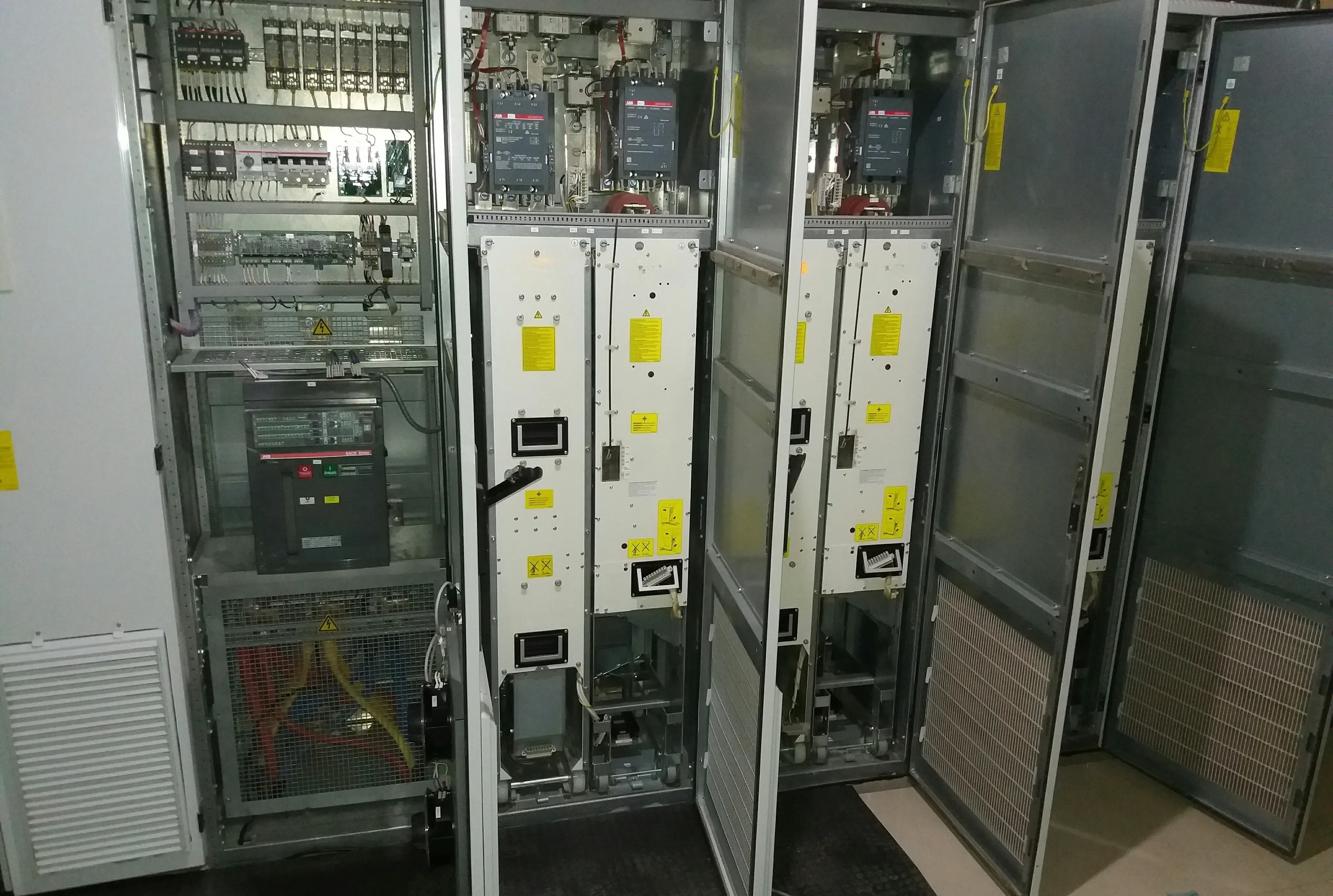
In utility-scale plants, central inverters in the 500 kW to 3.15 MW range will typically use press-pack or module-type IGBTs with voltage ratings of 1700 V or higher to accommodate 1000 V or 1500 V DC string systems. The IGBT modules are mounted on heatsinks with forced air or liquid cooling, because the switching losses they generate — the heat produced every time they turn on and off — need somewhere to go.
Thermal cycling is one of the dominant long-term ageing mechanisms observed in utility-scale IGBT modules. However, electrical overstress, gate driver faults, cooling system failures, contamination, surge events, and manufacturing defects can also contribute to field failures.
What Lives Alongside the IGBT — And Why It Matters
Before examining IGBT failure directly, it helps to understand what a central inverter’s power stage actually contains at the component level.
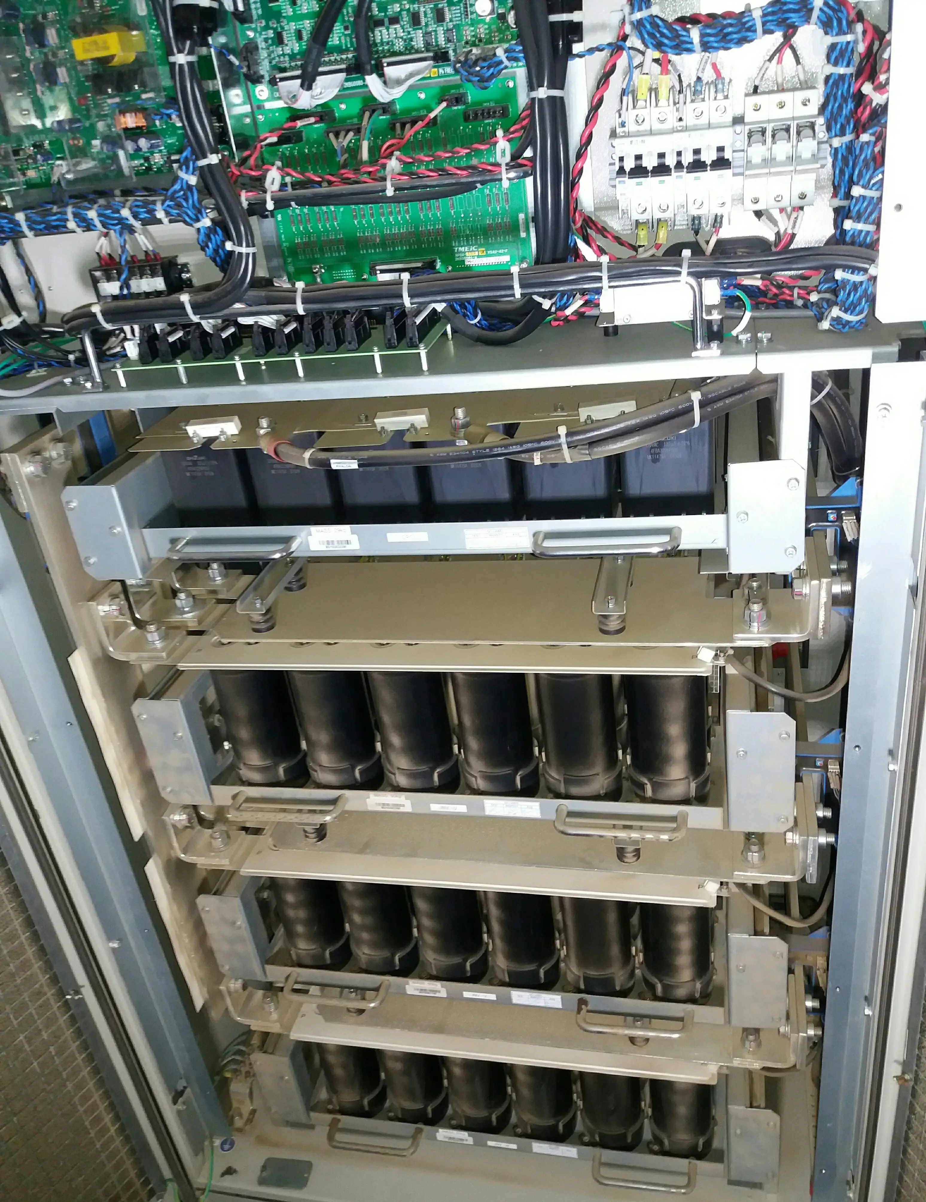
The DC link capacitors are the IGBT’s immediate neighbours. They maintain a stable DC bus voltage and absorb the voltage ripple that the switching action creates. When an IGBT module fails violently — short-circuit failure, for instance — the stored energy in these capacitors discharges instantly through the failure point. This is why IGBT failure events can cause secondary damage to adjacent components: the energy available at the DC bus at the moment of failure is substantial.
This matters for your post-failure assessment. When an inverter trips on an IGBT fault, do not assume the failure is isolated to the IGBT module itself. In the failure event documented later in this article, the gate driver PCB adjacent to the failed module showed burn damage consistent with the discharge event at the point of failure.
How IGBTs Fail in Field Conditions — The Mechanisms That Matter for O&M
Thermal stress is widely recognised as one of the most common long-term ageing mechanisms in utility-scale IGBT modules. Field investigations may also identify electrical overstress, gate driver malfunction, cooling deficiencies, contamination, or manufacturing defects depending on the failure event. The mechanisms discussed below focus on thermally driven degradation, which is the pathway most relevant to normal long-term plant operation.
Here is what happens physically:
Bond wire fatigue. The aluminium bond wires that connect the IGBT chip to the module’s terminal are attached using an ultrasonic bonding process. Every time the IGBT junction temperature rises and falls — which happens continuously as irradiance rises in the morning and drops in the evening — the bond wire and the chip beneath it expand and contract at slightly different rates. Over tens of thousands of thermal cycles, the bond wire lifts at its heel. Electrical resistance at the bond increases. The module begins running hotter than it should at the same power level. This is the start of the degradation curve.
Solder layer delamination. The IGBT chip is soldered to a ceramic substrate, which is in turn soldered to a copper baseplate that sits against the heatsink. As thermal cycles accumulate, micro-voids form in the solder joint. These voids reduce heat transfer between the chip and the heatsink. Thermal resistance increases. The junction temperature for a given power throughput now climbs higher than the datasheet predicts — and higher than the inverter’s temperature monitoring expects.
Gate oxide degradation. Under sustained high temperature and repeated high-voltage switching transients, the thin silicon oxide layer that forms the IGBT’s gate can degrade electrically. Threshold voltage shifts. The IGBT’s switching behaviour becomes less predictable. In some degradation pathways, this leads to increased leakage current or erratic gate response before complete failure.
These are not sudden events. They are accumulative. They develop over years. And in most cases, they produce measurable changes in inverter behaviour long before the protection system trips the unit offline.
The Three Failure Stages That Show Up in Plant Data
From field observations at utility-scale PV plants, many long-term IGBT degradation events can be interpreted as progressing through three practical stages. This is an engineering framework for understanding plant behaviour rather than a formal industry classification — the exact progression depends on inverter design, operating conditions, and the specific failure mechanism involved. O&M teams that are not tracking inverter efficiency continuously tend to miss the first two stages.
Stage 1: Silent Efficiency Degradation
As bond wire fatigue and solder delamination progress, the IGBT module’s internal resistance increases. This manifests as slightly higher conduction and switching losses — more of the DC input energy is being converted to heat inside the module rather than passed through to the AC output.
The consequence is a marginal but measurable decline in the inverter’s DC-to-AC conversion efficiency. On a correctly instrumented plant, this shows up as the inverter’s efficiency, measured as AC power output divided by DC power input, trending downward relative to its own historical baseline at similar power levels.
The key phrase is “at similar power levels.” Inverter efficiency is load-dependent. A fair comparison requires matching the efficiency figures against comparable DC power input levels — not raw time-period averages, which will be dominated by irradiance variation. Track this at the plant level with our free Inverter Efficiency Dashboard — it allows batch comparison of DC-to-AC conversion efficiency across multiple inverters from uploaded SCADA data.
Detecting IGBT-specific degradation in efficiency data requires a longitudinal baseline for the same inverter: its efficiency tracked weekly or monthly at consistent load bands, showing a directional trend downward over time. A single day’s numbers cannot establish that trend — irradiance variation, ambient temperature, and data quality issues will dominate any single-day comparison. What you are looking for is not one day’s number. You are looking for a direction of travel on the same inverter across months.
Stage 2: Thermal Derating Events
As internal thermal resistance climbs, the junction temperature begins exceeding the inverter’s thermal management thresholds at lower and lower output power levels. The inverter’s protection logic responds by throttling output — reducing AC power to bring junction temperature back within limits. This is thermal derating.
From the outside, thermal derating looks almost identical to inverter clipping in your SCADA data. Both produce a flat plateau in the inverter’s AC power output curve. Both cause the inverter to stop tracking the irradiance curve upward at peak-insolation hours. The distinction is the cause: clipping is the DC array outrunning the inverter’s rated AC capacity — a design-driven limitation. Thermal derating is the inverter’s self-protection system limiting output because internal temperatures are too high for the power stage components. The distinction matters because inverter clipping is an expected, bounded, calculable loss — while thermal derating is a maintenance signal.
In SCADA data, you can usually distinguish the two by cross-referencing with inverter temperature logs:
- Clipping: AC power plateaus at rated capacity. Inverter temperature remains within normal operating range. DC power is clearly available — DC voltage and current both present at the inverter input.
- Thermal derating: AC power plateaus below rated capacity, or steps down progressively during peak hours. Inverter temperature is elevated — typically at or near the upper end of the operating range. The derating may worsen over the course of a clear summer day as the inverter accumulates heat.
During Stage 2, your plant’s Performance Ratio will show a measurable gap during peak-irradiance hours. The PR denominator — insolation — continues rising, but the AC output is artificially constrained. You can calculate this real-time efficiency gap using our Instantaneous PR tool. The CUF impact accumulates across every derating event throughout the operating month.
Stage 3: Hard Trip
Bond wire or solder fatigue eventually reaches a point where the IGBT module can no longer maintain electrical integrity under switching load. The failure mode at this point depends on what fails first — open-circuit failure (the bond wire breaks completely, the IGBT stops conducting) or short-circuit failure (the semiconductor layer breaks down under voltage, creating a low-impedance path between collector and emitter).
Short-circuit failure is the more energetic of the two. The stored energy in the DC link capacitors discharges through the failure point. In a 1 MW inverter with a DC bus at 1000 V, the energy available at the capacitor bank at the moment of failure can cause violent internal damage — PCB burn damage, arc traces, and in extreme cases, physical rupture of the module enclosure.
The image below is from a utility-scale central inverter failure event at a multi-MW plant. The IGBT module is visible from the front of the power stage drawer. The gate driver PCB to the left of the module shows carbonisation consistent with the discharge event at the point of failure.
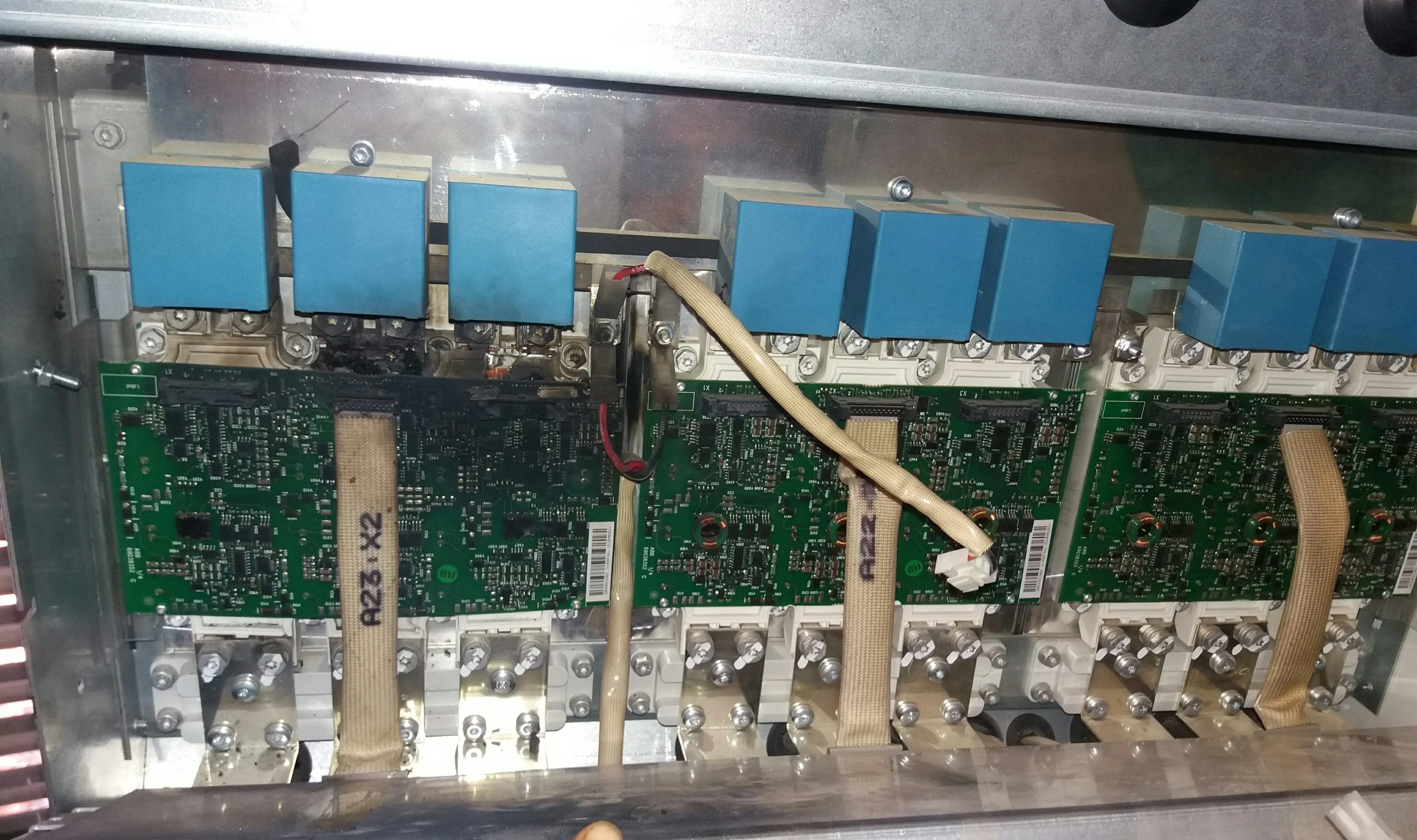
By the time this photograph was taken, the inverter had registered IGBT fault alarms intermittently for approximately two days prior to complete shutdown. The plant had logged the alarms, cleared them via remote reset twice, and allowed the inverter to resume operation. Both resets temporarily succeeded. On the third fault, the inverter did not recover.
The downstream damage extended to the gate driver board.
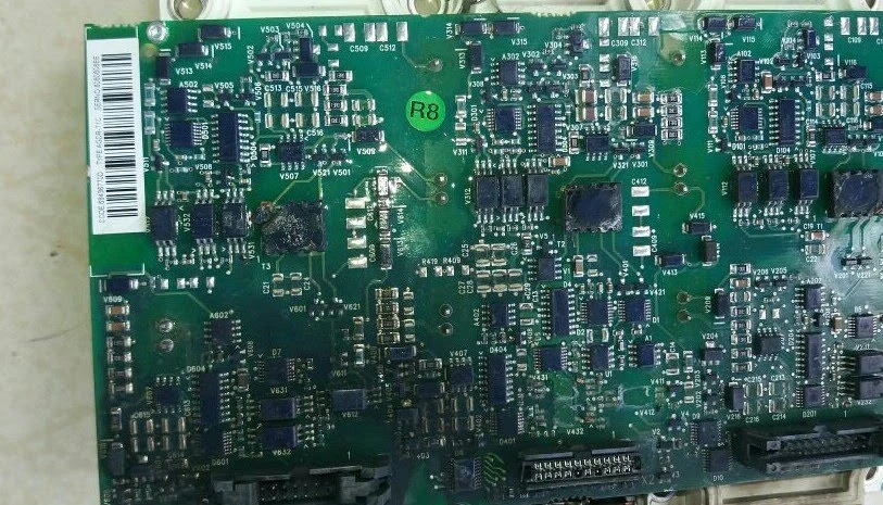
During the on-site investigation of this same failure, a Fluke infrared thermometer was used to take surface temperature readings across the gate driver PCB and the adjacent power stage assembly.
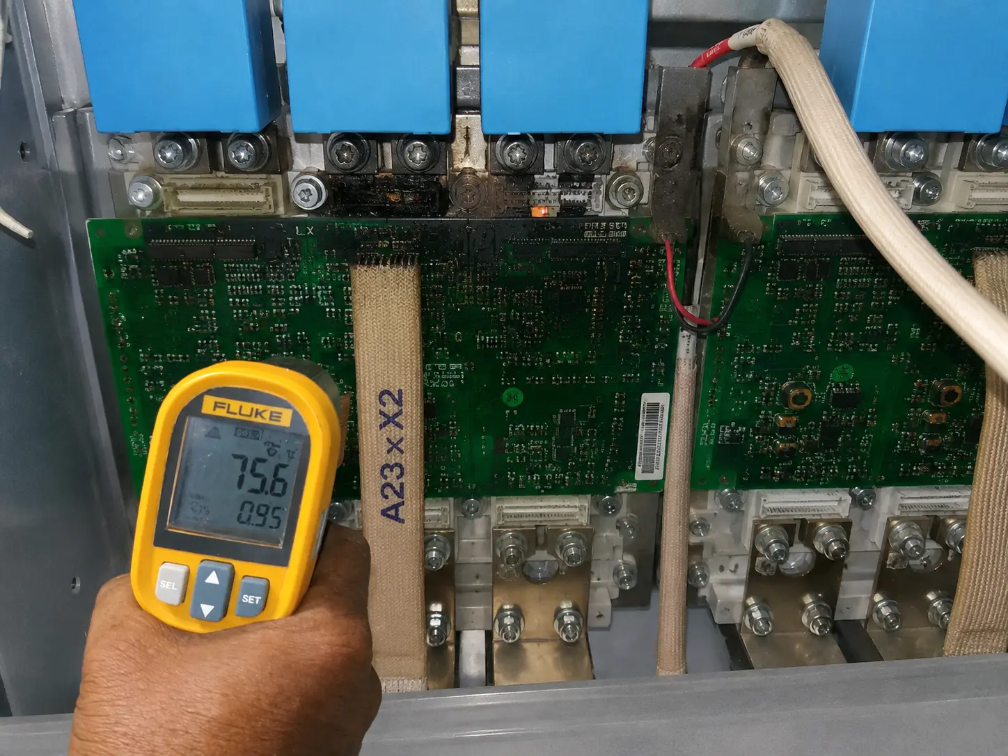
This reading illustrates a critical point that every O&M engineer handling inverter inspections needs to understand: 75.6°C is the PCB surface temperature. It is not the IGBT junction temperature.
The IGBT junction — the silicon die inside the module — is thermally isolated from any external measurement point by the module’s internal stack: die solder, ceramic substrate, baseplate solder, copper baseplate, thermal interface material, and heatsink. The thermal resistance across this stack, denoted Rθjc (junction to case) and Rθch (case to heatsink), determines the temperature difference between what the silicon experiences and what any external instrument reads.
In a new, healthy IGBT module, this thermal resistance is within the manufacturer’s specified range. In a module with accumulated bond wire fatigue or solder delamination — the conditions described in Stage 1 of this article — Rθjc has increased. The junction now runs hotter than it did when the module was new, at the same power throughput, even though every external measurement point shows the same temperature it always did. The inverter’s SCADA-logged cabinet temperature shows nothing unusual. A Fluke pointed at the heatsink or PCB shows nothing unusual. The thermal stress is invisible externally until it reaches a threshold that triggers either protection logic or physical failure.
This is precisely why IGBT thermal degradation is so consistently missed before a hard trip. The signal is inside the module. The instrumentation at the plant level measures the outside.
The Performance Impact: What IGBT Failure Costs in PR, CUF, and Efficiency
Inverter Efficiency
The DC-to-AC conversion efficiency loss from IGBT degradation is load-dependent and progressive. A degraded IGBT module that has increased its internal resistance by a measurable amount will increase conduction losses proportionally to the square of the current it carries. At rated load — which is when a 1 MW inverter is running at 900–1000 kW output — this penalty is at its highest.
To understand the order of magnitude: a Stage 1 efficiency degradation of 0.5 percentage points on a single inverter — the kind that can accumulate gradually from bond wire fatigue before any alarm fires — brings that inverter’s effective conversion efficiency from its healthy baseline to 0.5% below it. On a 1 MW rated inverter producing 800 MWh per month, that 0.5% drop represents approximately 4 MWh of additional monthly loss compared to its own baseline — generation that will not appear at the revenue meter and will not be recovered. The loss is silent, attributable to no single fault code, and invisible unless you are tracking efficiency trends longitudinally for that specific unit.
Performance Ratio
PR is directly suppressed by IGBT-related losses at each of the three failure stages:
Stage 1 (efficiency degradation): The inverter converts less of its DC input to AC output. For a fixed insolation and DC array input, AC generation at the meter is lower. PR = AC Energy ÷ (Installed Capacity × POA Insolation/1000) — the numerator falls while the denominator stays fixed. PR drops.
Stage 2 (thermal derating): During peak-irradiance periods when the inverter throttles output, the irradiance recorded by the plant’s weather station continues accumulating in the PR denominator. The AC output is artificially constrained. The PR gap during derating hours can be 3–8 percentage points below the plant’s true capability.
Stage 3 (complete trip): The inverter is offline. All irradiance during the outage period contributes to the PR denominator with zero contribution to the numerator. Plant and grid availability — calculated against irradiance-weighted hours per IEC 61724-1 — captures this correctly.
CUF and Energy Loss
The CUF impact depends on how long each stage persists before intervention. A 1 MW inverter offline for 48 hours during peak irradiance in a location receiving an average of 5 kWh/m²/day irradiance represents a generation loss on the order of 4,500–5,000 kWh. On a 10 MW plant with ten inverters, a single inverter offline for 48 hours reduces the monthly CUF by approximately 0.07–0.08 percentage points.
This appears small until you compound it with the Stage 1 and Stage 2 losses that may have been accumulating for weeks prior to the hard trip. Estimate the generation loss from an inverter failure event using our free Plant & Grid Generation Loss calculator.
What to Look For in Your Data — Before the Hard Trip
If you are managing a portfolio of central inverters, here are the specific data signatures worth tracking on a consistent basis:
Inverter efficiency trend over time. Pull AC power output and DC power input for each inverter at 15-minute intervals. Calculate the DC-to-AC efficiency at load levels between 60–100% of rated capacity (where the efficiency curve is relatively flat and comparable across days). Track the monthly average at this load band. A downward trend of 0.3% or more over three to four months on one inverter, while others hold steady, is worth investigating. Our Inverter Efficiency tool lets you upload SCADA data and compare efficiency across up to five inverters with per-device breakdowns.
Inverter temperature versus power output. Your SCADA should be logging inverter cabinet temperature or heatsink temperature. Plot inverter temperature against AC output power for a specific inverter across six months. If the temperature at a given power level is trending upward — the inverter runs 5°C hotter at 800 kW output than it did six months ago — thermal resistance is increasing. This is a degradation signal even before efficiency loss becomes detectable.
Recurring IGBT fault alarms with temporary clearance. If an inverter logs an IGBT fault that clears within minutes of logging, and this pattern repeats more than twice in a two-week period under similar irradiance conditions, do not continue remote-resetting without a physical inspection. The condition generating the fault is repeatable, which means it is structural.
Phase current imbalance. A partially failed IGBT — one leg degraded but not completely failed — can cause slight imbalance in the three-phase AC output currents. This is detectable in inverters that log per-phase current data. Compare Phase A, B, and C currents during stable, full-power operation. A consistent difference of more than 2–3% between phases on one inverter that is not present on others warrants investigation.
Power factor deviation. IGBTs control the reactive power output of the inverter through their switching pattern. Degraded IGBTs can produce subtle reactive power anomalies that show up as power factor deviation from the setpoint. If your SCADA logs power factor per inverter and one unit consistently deviates from its programmed setpoint while others do not, it is worth adding to the inspection list.
A critical caveat on efficiency data: What appears in the SCADA as inverter efficiency is typically calculated from the inverter’s own internal DC current and voltage sensors, plus the AC power measurement. Both sensor chains carry their own measurement uncertainty. Efficiency readings above 100% — physically impossible for any passive power conversion device — do appear in real plant data and are always a measurement artefact: calibration drift on the DC current sensor, a rounding error at low load during morning ramp or evening decline, or a data pipeline error. Before attributing a declining efficiency trend to IGBT degradation, verify that the underlying sensor calibrations are current. A trend caused by a drifting current transducer is not the same problem and has a completely different corrective action.
Although MPPT algorithms determine the operating point of the PV array, the power requested by that algorithm still passes through the inverter’s IGBT switching stage before reaching the AC output terminals. A degrading IGBT power stage can therefore reduce DC-to-AC conversion efficiency even when MPPT tracking remains correct — the two are independent failure paths. Our article on What Is MPPT in Solar Inverters explains how the MPPT control algorithm and the IGBT power conversion stage interact inside a solar inverter.
Replacement and Post-Failure Considerations
Once an IGBT module fails in a central inverter, replacement requires:
- Confirming the failure mode — open-circuit versus short-circuit — to assess secondary damage extent
- Inspecting adjacent IGBT modules and gate driver boards under load testing before returning the unit to service. Electrical stress from a short-circuit failure event can damage adjacent components that appear visually intact
- Verifying thermal paste application and heatsink contact on the replacement module — inadequate thermal interface material is one of the most common causes of early re-failure in replacement modules
- Checking DC link capacitor health, as these absorb significant stress during a violent failure event
- Updating the maintenance log with the exact fault alarm sequence, timestamps, and environmental conditions at the time of failure — this longitudinal record is what makes future pattern recognition possible across your fleet
On the Plant & Grid Availability calculator, log the inverter offline period against the irradiance-weighted hours during that period. This gives you the correct availability figure for that inverter for the reporting month — and keeps it out of the unexplained loss bucket where it would distort your PR root-cause analysis.
Key Takeaways
- IGBTs are the power switching devices at the core of every solar inverter’s DC-to-AC conversion stage. Every kilowatt-hour your plant generates passes through them.
- Failure in field conditions is driven primarily by thermal stress — bond wire fatigue and solder layer delamination that accumulate over tens of thousands of daily thermal cycles.
- IGBT degradation progresses through three stages before hard failure: silent efficiency decline (Stage 1), thermal derating events (Stage 2), and complete trip (Stage 3). Most O&M monitoring only detects Stage 3.
- Stage 2 thermal derating produces a flat-top power curve in SCADA data that is frequently misclassified as inverter clipping. Cross-referencing with inverter temperature logs distinguishes the two.
- Efficiency loss from IGBT degradation is load-dependent and accumulates progressively — detecting it requires tracking the same inverter’s efficiency at consistent load bands over months, not comparing a single day’s numbers.
- A recurring IGBT fault alarm that clears with remote reset and returns within the same week is a hardware condition, not a transient event. Continuing to reset without physical inspection risks escalating a controlled replacement to a more damaging failure.
- An IR gun reading on a PCB or heatsink surface does not tell you the IGBT junction temperature. The thermal gradient across the module’s internal stack — which widens with bond wire fatigue — is invisible to external instruments.
- Post-failure availability loss should be logged against irradiance-weighted hours for correct IEC 61724-1 compliant availability calculation.
Frequently Asked Questions
What is an IGBT in a solar inverter?
An IGBT (Insulated Gate Bipolar Transistor) is the primary power switching device in a solar inverter’s conversion stage. In a central inverter, multiple IGBT modules are arranged in a three-phase bridge configuration. Their role is to switch the DC power from the PV array at high frequency under the control of the inverter’s gate driver circuitry. The exact switching frequency varies by inverter topology and manufacturer design, but the objective is the same: produce a grid-synchronised AC waveform with high DC-to-AC conversion efficiency and within the harmonic limits set by the applicable grid code. Every ampere of DC current generated by the PV array passes through the inverter’s IGBT bridge before being converted into AC power.
How does IGBT failure affect Performance Ratio?
IGBT degradation suppresses PR through two mechanisms before hard failure: Stage 1 efficiency loss reduces AC output at a given irradiance, lowering the PR numerator; Stage 2 thermal derating caps AC output during peak irradiance hours while irradiance continues accumulating in the PR denominator. After a hard trip, the complete inverter outage eliminates the unit’s contribution to generation entirely while irradiance hours continue accumulating. All three stages reduce PR.
Can I detect IGBT degradation before failure using SCADA data?
Yes, but it requires tracking the right parameters consistently over time. The most useful signals are: inverter efficiency trend at comparable load levels over months (not single-day comparisons); inverter temperature at a given power output level trending upward over months; recurring IGBT fault alarms that clear and return; and phase current imbalance in per-phase logging. A single day’s efficiency numbers cannot diagnose IGBT-specific degradation — you need a longitudinal baseline for the same inverter.
What is the difference between IGBT thermal derating and inverter clipping?
Both produce a flat-top plateau in the inverter’s AC power output curve. Clipping happens when the DC array output exceeds the inverter’s rated AC capacity — a design-driven, expected condition that occurs at rated power. Thermal derating happens when the IGBT junction temperature exceeds safe limits and the inverter throttles output to protect the power stage — this occurs below rated capacity and is correlated with elevated inverter temperature readings. Clipping is bounded and predictable. Thermal derating is a maintenance signal.
What components should be replaced after an IGBT failure?
The failed IGBT module must be replaced. The gate driver PCB associated with the failed module should be tested and replaced if there is any evidence of thermal or electrical stress — do not assume it is undamaged based on visual inspection alone. If the failure was a short-circuit event, the DC link capacitors on the same bus segment should be tested before returning the inverter to service. Adjacent IGBT modules in the same phase leg should be load-tested, as they may have experienced elevated electrical stress during the failure event.
Should I reset an inverter after an IGBT fault alarm?
A single IGBT fault that clears and does not return for several days under similar conditions may be a transient. If the alarm returns within the same operating week at similar irradiance levels, it is almost certainly a developing hardware condition. Remote-resetting without physical inspection risks escalating the failure from a controlled module replacement to a more damaging event. Two or more returns within a seven-day period warrants an on-site inspection before the next reset.